# D+7A I/O connector pinouts
# Original S-100 Cromemco D+7A I/O connector
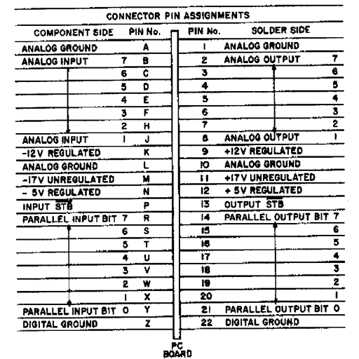
The following diagram is from the original Cromemco D+7A I/O documentation
# S-132 D+7A I/O connector
The S-132 D+7A I/O 40-pin (female) connector closely matches the original Cromemco D+7A I/O 44 position edge connector providing most of the same Analog and Digital inputs and outputs in the same configuration. Mainly it differs in the voltages that are (or are not) provided around the middle of the connector.
| ESP32 Side | Pin No. | Pin No. | LM7805 Side | ||
|---|---|---|---|---|---|
| Top | Top | ||||
| Analog Ground (1) | A | 1 | Ground | ||
| Analog Input (2) | 7 | B | 2 | N/C | 7 |
| 6 | C | 3 | N/C | 6 | |
| 5 | D | 4 | N/C | 5 | |
| 4 | E | 5 | N/C | 4 | |
| 3 | F | 6 | Analog Output (3) | 3 | |
| 2 | H | 7 | N/C | 2 | |
| 1 | J | 8 | Analog Output (3) | 1 | |
| Voltage Ref. (4) | H | 9 | Voltage Ref. (4) | ||
| +5V DC Regulated | N | 10 | +5V DC Regulated | ||
| Input _STB (5) | P | 11 | Output _STB (6) | ||
| Digital Input Bit (7) | 7 | R | 12 | Digital Output Bit (8) | 7 |
| 6 | S | 13 | 6 | ||
| 5 | T | 14 | 5 | ||
| 4 | U | 15 | 4 | ||
| 3 | V | 16 | 3 | ||
| 2 | W | 17 | 2 | ||
| 1 | X | 18 | 1 | ||
| 0 | Y | 19 | 0 | ||
| Ground | Z | 20 | Ground | ||
| Bottom | Bottom |
# Notes:
Analog Groundis isolated fromGround- for most use cases you should tie it to
Ground
- for most use cases you should tie it to
Analog Input 1 to 7- these are digitized by the MCP3008 ADC
- typically
0VtoVoltage Ref. Vfor signed input port values of-128 to 127 - see the MCP3008 ADC data sheet for exact specifications
- There are only two (2) analog outputs
Analog Output 1andAnalog Output 3- because there are only two (2) DACs on the ESP32
- these are
0Vto+3.3V(or slightly between these limits) for signed output port values of -128 to 127 - you can map any of the Analog Output ports to either of these two (2) DACs (see config guide for D+7AIO settings)
- it's 1 & 3 because that is what the Cromemco JS-1 Analog Joysticks used for audio
Voltage Ref.is the V.Ref on the MCP3008 ADC- for most use cases you should tie it to
+5V Regulated
- for most use cases you should tie it to
Input _STB(active low) isn't implemented - because... reasons.Output _STB(active low) is implemented- as a working example: this is used on the Parallel Printer interface as the parallel output data strobe
Digital Input Bits 0 to 7- these are buffered by the 74HC165 with a
+5V DCregulated supply forVcc - typically
> 3.15V = 1and< 1.35V = 0 - see the 74HC165 data sheet for exact specifications
- these are buffered by the 74HC165 with a
Digital Output Bits 0 to 7- these are driven by the 74HC595 with a
+5V DCregulated supply forVcc - typically
0V = 0and+5V (Vcc) = 1 - see the 74HC595 data sheet for exact specifications
- these are driven by the 74HC595 with a